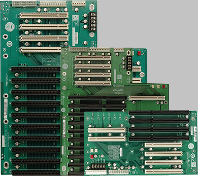
Backplane (BP)
Large-format, high-layer-count backplanes for high-speed interconnection in communication and server racks.
- 类型/Type: 背板 Backplane
- 工艺/Craft: 高层数通孔、背钻、混压
15 product lines covering backplanes, line cards, server and antenna boards, HDI, hybrid, heavy-copper and metal-backed PCBs — up to 64 layers, 3–12 oz copper, blind/buried vias, back-drilling, PTFE and ceramic-filled materials, cavity and step boards.
Large-format, high-layer-count backplanes for high-speed interconnection in communication and server racks.
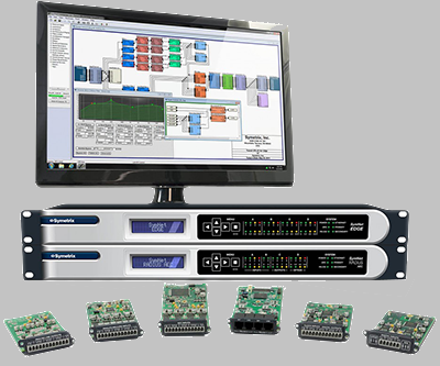
Printed circuit boards for line cards and daughter cards in communication equipment.
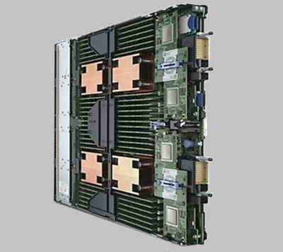
Boards for server mainboards and compute boards — up to 40-layer through-hole, up to 24 x 42 inch panel size.
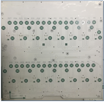
RF boards for base-station antennas, filters and power amplifiers; PTFE and ceramic-filled materials.
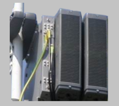
High-density interconnect boards with blind/buried vias and fine-line capability for compact, high-performance devices.
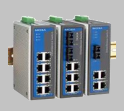
Multi-material hybrid boards — FR4 / PTFE / ceramic, full-surface or local lamination.
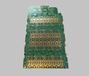
Metal-backed (heat-sink) PCBs for high-power devices: copper block bonding, embedded copper, post-bonding.
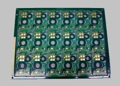
Heavy copper PCBs, 3 oz to 12 oz copper, up to 20 layers, for high-current and power applications.
Automotive electronics: braking, steering, powertrain, e-motor, battery management, inverters, ADAS, body electronics, infotainment and navigation.
Power supply equipment: DC-DC converters and high-end equipment / computer power supplies.
High-end servers and industrial computers: up to 40-layer through-hole boards, panel size up to 24 x 42 inch.
Wireless telecom infrastructure: base stations (4G / 5G / WiMax / LTE), antennas, filters and power amplifiers.
Core network (wired): high-end routers, switches and storage for cloud computing.
Semiconductor: custom designs for chip makers, emulators, ATE test, burn-in test, wafer test carrier boards and probe-card carriers.
Industrial: motion control, temperature and humidity control, factory automation, construction machinery and office equipment.